
Strongly correlated materials can change their resistivity from infinity to zero with minute changes in conditions. Now, researchers have fabricated a flexible organic “correlated” transistor that makes it possible to control the effective pressure and doping level by bending the substrate and changing the gate voltage, respectively. This device allows researchers to switch superconductivity on and off by using appropriate combinations of the two parameters, in a way that could lead to future quantum simulators.
In the strongly correlated materials such as cuprate high-temperature superconductors, superconductivity can be controlled either by changing the number of electrons or by changing the kinetic energy, or transfer energy, of electrons in the system. Although a large number of strongly correlated materials have been examined with different parameters to understand the mechanism of superconductivity, the range of parameter control is always limited. A versatile experimental method to achieve simultaneous control of the number and the transfer energy of the electrons has been long desired.
A flexible electric-double-layer transistor (EDLT), or “correlated” transistor, composed of an organic strongly correlated material was constructed (Fig. 1) by researchers at RIKEN, Institute for Molecular Science (IMS), Nagoya University and Toho University. The number of electrons can be controlled by gate voltages of the EDLT, and the transfer energy of electrons can be controlled by bending the EDLT substrate. They found that the system changed from an insulator to a superconductor in both cases of increasing and decreasing electron numbers. Conditions for these superconducting states in the above two cases, however, were found to be fundamentally different. In addition, another superconducting state emerged when the substrate was bent. The present result was published online on Science Advances on May 10, 2019.
Researchers fabricated the EDLT using a crystal of the organic strongly correlated material made of BEDT-TTF (bis(ethylenedithio)tetrathiafulvalene) molecules (Fig. 1). By applying the gate voltage on to the surface of the crystal, the number of electrons can be increased (electron doping) and decreased (hole doping). This EDLT device is flexible, and the transfer energy can be controlled by applying mechanical force (strain) from the back side of the EDLT. The researchers successfully controlled superconductivity in an identical sample, by precisely changing both the gate voltage and the strain.
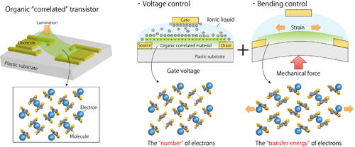
Figure 1. Schematics of EDLT
Before applying perturbations by the mechanical pressure or the electric gate voltage, the organic correlated material stays in an insulating state since the electrons seat themselves snugly in their “reserved seats” at the molecules. After the gate voltage is applied, the number of electrons changes and gives rise to vacant (hole-doped) or standing (electron-doped) seats. The mechanical pressure causes the change in the distance between the seats. The appropriate combination of these perturbations switches the material to be a superconductor.
Figure 2 shows the regions of superconducting states. The abscissa shows the gate voltage, which corresponds to the number of doped electrons. The ordinate shows the strain applied to the device by bending. With going down along the ordinate, the electrons move more easily because the kinetic energy of electrons increases. The region of the insulating state (red) is surrounded by the regions of superconducting states (blue). Two superconducting regions of the left and the right sides of the insulating region are significantly different in shape on Fig. 2. Especially the superconducting state appeared with an increasing number of electrons (the right side on Fig. 2) shows remarkable behavior that the state appeared suddenly with a few percent increase of the number of electrons and disappeared with an addition of excess electrons. The superconducting states can be obtained both by increasing and by decreasing electron numbers. However, the features of the two states are found to be fundamentally different.
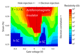
Figure 2.Phase diagram
Resistivity is shown by colors. The insulator region (red) is surrounded by the superconducting regions (blue). The shapes of the insulating and superconducting regions differ between the negative and positive ranges of the gate voltage. The shape of the electron-doped superconducting region (e-SC) is found to be quite anomalous.
The two-dimensional phase diagram (Fig. 2) was thus obtained using the single sample. The diagram shows the nature of the superconducting phase transition, which has been anticipated from data collected from many different samples before this device appears. Therefore this newly developed experimental method accelerates to obtain the phase diagrams. More fundamentally, drawing the full phase diagram from the same sample enables us to obtain more reliable results regardless of the effects of impurity and of difference in crystal structures.
This experimental method can apply to various organic strongly correlated materials. One interesting example is the quantum spin liquid in which the directions of electron spins are moving randomly even at 0 Kelvin. Experiments on the quantum spin liquid will reveal the relationship between superconductivity and magnetism (arrangement of electron spins). It is also notable that the phase diagram of strongly correlated electron system is a significant target of quantum simulators. The present result provides one possible standard solution for those newly developing calculation methods.
Information of the paper
Authors: Yoshitaka Kawasugi, Kazuhiro Seki, Satoshi Tajima, Jiang Pu, Taishi Takenobu, Seiji Yunoki, Hiroshi M. Yamamoto, and Reizo Kato
Journal Name: Science Advances
Journal Title: “Two-dimensional ground-state mapping of a Mott-Hubbard system in a flexible field-effect device”
DOI: 10.1126/sciadv.aav7282
Financial Supports
Grant-in-Aid for Scientific Research
15K17714, 16H06346, 16H04140, 26102012, 25000003
Contact Person
Professor Hiroshi Yamamoto
TEL/FAX: +81-564-55-7334 / +81-564-55-7325
E-mail: yhiroshi_at_ims.ac.jp
*Please replace the "_at_" with @
1034
