Research Theme
Nanostructure fabrication, optical property control, and photonic functionalization of atomic-layer materials
Keywords
Semiconductors, two-dimensional materials, photophysical properties, optical science
Modern electronic devices are approaching their miniaturization limits, necessitating innovative solutions through the integration of optical and quantum effects. Our research group focuses on atomic layer materials, particularly transition metal dichalcogenides (TMDs), which exhibit remarkable optical properties due to their single-atom thickness.
These materials possess direct bandgaps with strong light-matter interactions and unique electronic properties stemming from their extreme two-dimensionality. By stacking different atomic layers through van der Waals forces, we can create artificial heterostructures. In these structures, excitons--bound pairs of electrons and holes generated by photoexcitation--become spatially confined within periodic moiré potentials.
Our team has successfully observed exciton localization phenomena in WSe2/MoSe2 heterostructures induced by moiré potentials. Through detailed investigations of interlayer exciton formation and their optical responses, including circular polarization characteristics and quantum coherence measurements, we continue to elucidate the quantum states of moiré excitons. Currently, we are advancing this research by developing nanofabrication techniques for atomic layer materials and precisely controlling light-matter interactions to explore novel optical phenomena and functionalities.
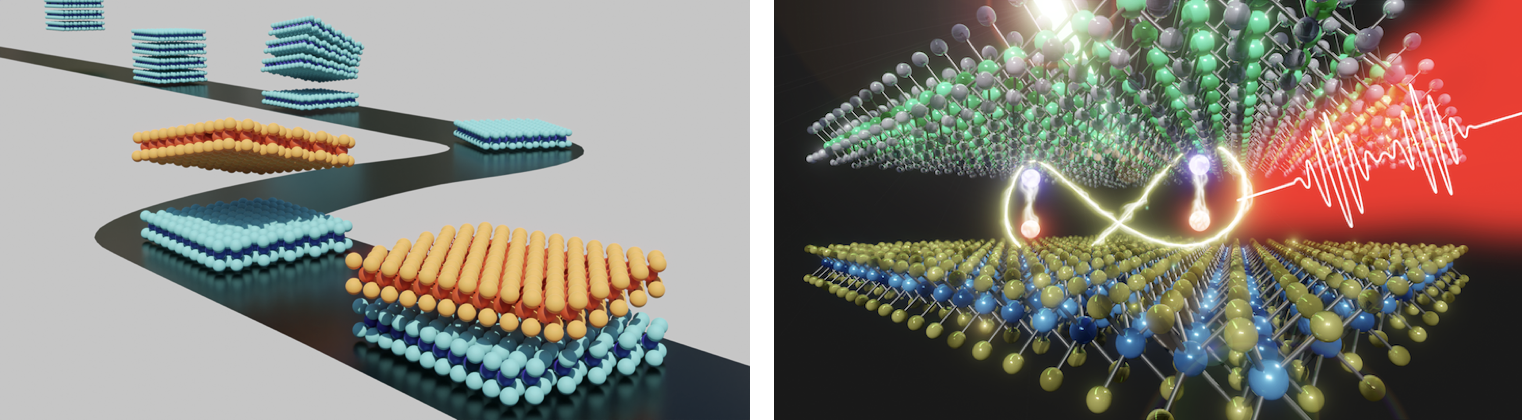
Left: Schematics of nanofabrication process for atomic-layer materials. Right: Visualization of quantum optical phenomena emerging from the engineered atomic-layer nanostructures
nanostructures
Selected Publications
- "Quantum coherence and interference of a single moiré exciton in nano-fabricated twisted monolayer
semiconductor heterobilayers" H. Wang, H. Kim, D. Dong, K. Shinokita, K. Watanabe, T. Taniguchi, and K.
Matsuda, Nat. Commun. 15, 4905 (2024).
- "Valley Relaxation of the Moiré Excitons in a WSe2/MoSe2 Heterobilayer" K. Shinokita, K. Watanabe, T.
Taniguchi, and K. Matsuda, ACS Nano 16, 16862 (2022).
- "Resonant Coupling of a Moiré Exciton to a Phonon in a WSe2/MoSe2 Heterobilayer" K. Shinokita, Y.
Miyauchi, K. Watanabe, T. Taniguchi, and K. Matsuda, Nano Lett. 21, 5938 (2021).
- "Continuous Control and Enhancement of Excitonic Valley Polarization in Monolayer WSe2 by Electrostatic
Doping" K. Shinokita, X. Wang, Y. Miyauchi, K. Watanabe, T. Taniguchi, and K. Matsuda, Adv. Funct. Mater.
29, 1900260 (2019).